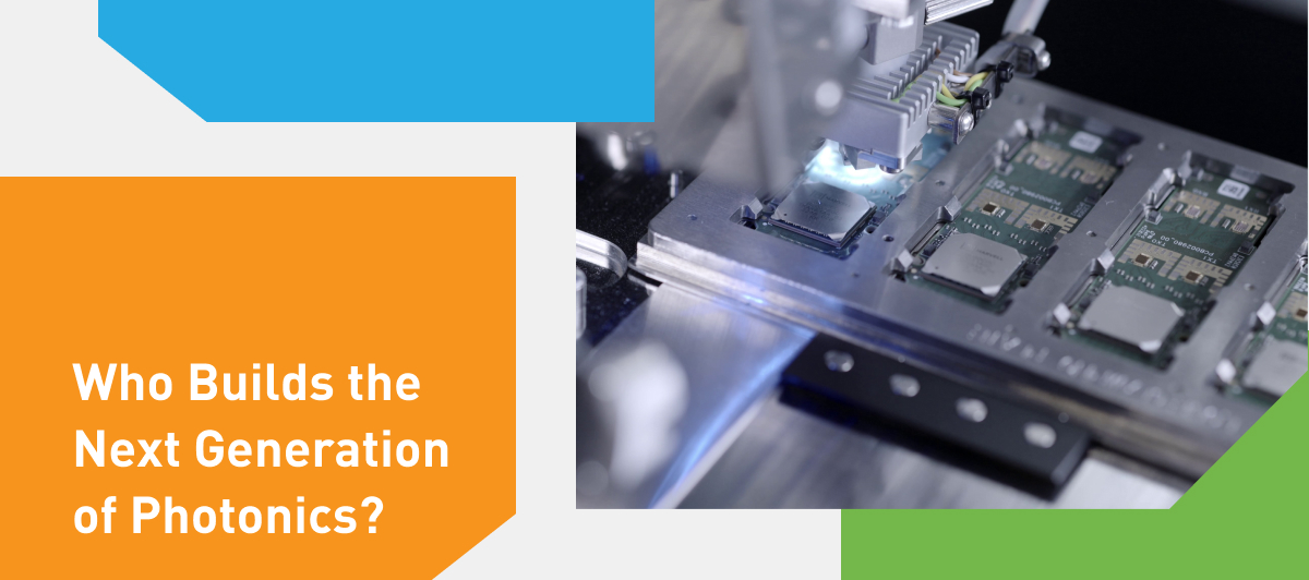
Co-packaged optics is already shipping in its first generation. The open question isn’t whether it can be built, it’s at what yield. Early CPO yields still trail the level where the economics beat pluggables, and that gap gets closed in production, where even carefully designed architectures throw up problems that only surface in assembly.
Finetech works at exactly that point. We make sub-micron die bonding equipment for the transfer from R&D to production, where most photonic processes quietly break. What follows is what that transfer actually turns on: accuracy, bonding method, and the handoff between development and production.
The assembly decides the device now
Performance comes from integration, not from shrinking a single chip: chiplets, 2.5D and 3D stacking, co-packaged optics. CPO is the sharpest case. It packs the optics against the compute chip, cuts the electrical path to almost nothing, and delivers more bandwidth at lower power. That closeness demands precise assembly.
The parts that will define the market won’t be buildable without it: AI accelerators, high-bandwidth memory, optical engines. Treat packaging as a back-end afterthought and you get locked out.
Three things decide whether a process scales. Miss one and it stalls, however well it ran in the lab:
- Accuracy, the right accuracy for the job, held on every unit
- Flexibility, one flow across many bonding methods
- Repeatability, the thousandth bond matches the first
The right accuracy, and the right alignment strategy
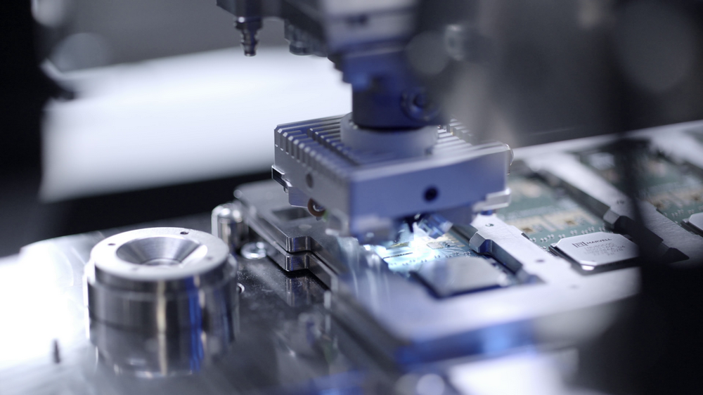
Not every job needs the tightest tolerance. For much of today’s photonics work, passive optical alignment is the right tool: camera-based recognition, repeatable positioning, what you see is what you bond. The numbers that ship prove it, 2 to 4 µm for fiber couplers, laser diodes, VCSEL and photodiode arrays.
Advanced packaging shifts the requirement. A laser aligned to a photonic IC in the lab drifts at volume, as small deviations and thermal effects pile up across many units. Static placement stops being enough. Holding the coupling then means measuring it live, in six or twelve axes as the component is positioned, so it holds on every unit and not just the first.
Read the requirement right. That’s half the job.
Hybrid bonding pushes density further, and forgives less
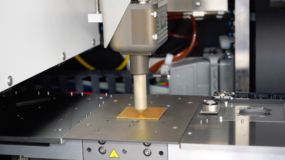
Direct die-to-die connections at extreme fine pitch, no bump between them. The upside: better signal integrity, lower power, higher density. The catch: it’s the least forgiving process there is. It demands high flatness, co-planarity, and clean, activated surfaces, with the vertical axis mattering as much as the lateral one. That last requirement is why surface preparation belongs inside the bonding sequence: in-line plasma activation right before the bond, with no window for the surface to degrade. What hybrid bonding solves at volume, photonic integration inherits. Finetech offers it as part of its bonding portfolio.
Not a handshake. A handoff.
Production rarely fails inside a single step. It fails at the interface between development and manufacturing, when the two run on different systems, software and logic. Too often that interface is a handshake: design finishes its part, hands it over, and from there it’s a manufacturing problem. Those gaps multiply as integration deepens. Talk to the people moving these processes into production and it comes back to the same thing: making it work isn’t the problem, doing it in fewer steps is.
A handoff is different. The ball goes straight from one hand to the next and can’t drop:
- Design knows the manufacturing requirements from the start
- Manufacturing takes the process over without a break
That’s what we’ve done with many customers, carrying a process from manual prototype onto automated production with no second development loop. Ultra Communications, building optical transceivers for rugged environments, made exactly that move.
Continuity is the fix, and it has to be designed in
Same hardware principles, bonding technologies, software and recipes from prototype to volume. Then a validated process transfers without a second loop, learning cycles shorten, and yield settles earlier.
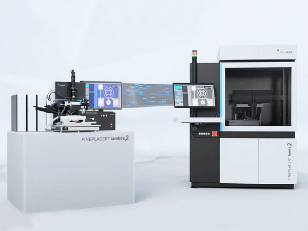
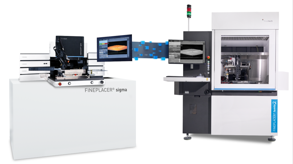
That’s the point of the FINEPLACER® platform. Every machine on it shares the same software, process logic and manual control, so a process can be developed on a tabletop or an automated system, whichever fits your business case, budget and timeline, and moves up without being re-learned. It’s the same platform behind three very different devices, all on one route from prototype toward volume:
- Polar Light Technologies, microLEDs down to 300 nm bonded by room-temperature cold compression at sub-micron XYZ alignment and ultra-low force, over 85% initial yield
- PHIX Photonics, VCSELs, photodiodes and TIAs integrated onto PICs by laser-assisted thermocompression at the wafer level, from prototype to high volume
- Peak Quantum, 3D-stacked superconducting qubits joined by indium flip-chip bonding with sub-micron accuracy and co-planar bondlines, now in the EU SUPREME pilot line
The flexibility matters most while the technology is still moving: product requirements shift, new market trends and technology drivers land mid-cycle. Develop and ramp early production on the same platform, and you can absorb those changes instead of re-qualifying from scratch every time the target moves.
For full-rate production, a dedicated in-line, wafer-level system is in development, built to carry a qualified process to volume at 12-inch scale.
Plan packaging from the first design
Even careful designs throw up problems that only surface in assembly. So define wafer layout, interconnect design and assembly architecture with bonding requirements in view. Get design and packaging engineers talking early, and you avoid the re-spins and yield losses that otherwise show up two years later.
For advanced packaging, scalability is a design constraint from the first prototype. Packaging is becoming the first decision in the flow.
So who gets to build the next generation of photonics, quantum and advanced microsystems? Whoever masters the transfer from lab to volume, the handoff where design and manufacturing meet without a break. The best chip doesn’t decide it. The package does, and it’s the first decision now, not the last.